Global high-mix volume high-speed PCBA manufacturer
9:00 -18:00, Mon. - Fri. (GMT+8)
9:00 -12:00, Sat. (GMT+8)
(Except Chinese public holidays)


Global high-mix volume high-speed PCBA manufacturer
9:00 -18:00, Mon. - Fri. (GMT+8)
9:00 -12:00, Sat. (GMT+8)
(Except Chinese public holidays)


HomePage > Blog > Knowledge Base > How to Design a Flex PCB: A Comprehensive Guide
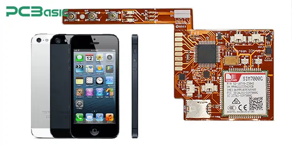
Modern electronic products are becoming increasingly thinner, lighter, and more powerful. Among them, flexible circuit boards play an important role. Flexible PCB can be bent and folded, and can adapt to complex spatial structures and dynamic working environments, which makes it the best choice for thin and light electronic products. The application of flexible PCBs is very extensive. It is widely applied in fields such as wearable devices, smartphones, automotive electronics, medical equipment, and aerospace.
However, designing a flex PCB with high reliability and high manufacturing yield is not simple. In the following article, we will systematically explain to you how to design a flex PCB. This article will help you create flexible circuit boards that are functionally stable, manufacturing-friendly and have excellent performance.

A flex PCB is a type of circuit board manufactured using flexible substrates such as polyimide or polyester. It can be bent, twisted and folded without damaging the conductive circuit. This flexibility enables electronic systems to adapt to compact, curved or moving structural environments. This flexibility is what sets flexible PCBs apart from rigid designs.
PCBs are generally classified into three types based on mechanical characteristics:
Rigid PCB: A hard structure that cannot be bent.
Flex PCB: Fully bendable and highly adaptable;
Rigid-Flex PCB: Balancing structural and flexible requirements.
This article mainly explains flexible circuit boards (flex PCB). Flexible circuit boards are widely used in scenarios with limited space or extremely high reliability requirements, such as smartphones, wearable devices, automotive electronics, medical implant devices, and aerospace systems. They have advantages such as lightweight structure and better seismic performance, making them an ideal choice for modern high-performance electronics. So, how do you design a flex PCB with good performance and stable functions? In the next section, we will gradually introduce the design process of flexible PCBs to you.
A successful flex PCB design requires careful consideration of material properties, mechanical structure, electrical performance, and manufacturability.

Any excellent flex PCB design begins with a clear definition of requirements. Different application devices have different requirements for circuit boards. So before designing the flex PCB, you need to think first whether the flex PCB will be used in wearable devices, medical implants, or automotive sensors. During the early stage of design, it’s essential to clarify the following parameters: ① Number of layers and required flex PCB thickness ② Static or dynamic bending ③ Working environment (temperature, humidity, vibration, etc.) ④ Lifespan and bending cycle requirements ⑤ Electrical performance targets such as impedance control and electromagnetic compatibility (EMC). These early decisions will become the key guiding basis throughout the entire flex PCB design process.

The second step is the selection of materials. The choice of materials directly affects flexibility, durability and cost. In most flexible circuit boards, common materials include:
Base material: It is recommended to choose polyimide (PI) as it has excellent heat resistance and mechanical flexibility. Of course, other materials are also acceptable, but PET material is not recommended for use in high-temperature or dynamic bending environments, because of its poor thermal performance.
Coverlay: Using coverlay instead of the traditional solder mask layer is more suitable for curved areas. Because traditional liquid solder mask materials are prone to cracking on flexible boards, they are not recommended for use.
Adhesive: Used for interlayer bonding or reinforcing panels. It is recommended to choose acrylic or epoxy adhesives with good heat resistance and high flexibility.
Copper foil: Rolled annealed copper (RA) is recommended and more suitable for bending.
The above are some suggestions on material selection. Of course, when conducting flex PCB design, the selection of materials, most importantly, should be based on the specific application requirements of the product.

A good FPC design must be based on a reasonable laminated structure. Only in this way can the electrical performance and mechanical stability of the flex PCB be guaranteed. Typically, single-layer flex PCBs are suitable for simple, static and low-budget applications. Double-layer or multilayer flex PCBs are suitable for circuits with complex traces or those requiring shielding. The rigid-flexible combined PCB integrates the rigid area and the flexible area into a whole, making it more suitable for applications that require a balance between structure and flexibility.
It is recommended to use stack-up simulation tools during planning. Or communicate with the flex PCB manufacturer to determine the appropriate structural design.

After the materials and structure are determined, the schematic design stage can be entered. When designing the schematic diagram, the following mainstream flex PCB design software can be used as aids: Altium Designer, KiCad (open source), Cadence Allegro, and Mentor Graphics PADS. Note: The schematic should include all signal, power, and ground wire connections, and preset functional modules such as high-speed signals, differential pairs, and filtering.

At this stage, it is necessary to strictly abide by the flex PCB design rules to ensure the electrical and mechanical reliability of the flexible area. The following are some of our suggestions:
① It is recommended to use arcs or 45-degree bends and avoid sharp-angle routing. Note: 90-degree turns are prohibited.
② Widen the wiring in the curved area. This helps distribute stress evenly and improves durability.
③ Use grid ground layer to enhance flexibility and reduce the risk of copper cracking.
④ Do not place vias in curved areas.
⑤ Adopts tear drop treatment and anchoring vias to reinforce the solder pads.
⑥ Meet the minimum bending radius requirement. (Generally, for dynamic applications, it is 10 times the plate thickness.)
In addition to these suggestions, we also recommend referring to the IPC-2223 standard and combining it with the flex PCB design and assembly guidelines provided by the manufacturer.

Before completing the wiring, it is best to conduct a DFM collaborative review with the flex PCB manufacturer. Special attention should be paid to the position and thickness of the reinforcing board, connector type (such as ZIF pads), soldering and assembly tolerances, panelization method, etc.
After completing the DFM review, the design rule check and electrical rule check are then carried out through the flex PCB design software. Key inspection points: line width/line spacing, pad size and spacing, window opening position of the coverlay, and keeping a blank area (Keep-out) in the bending area. For high-speed flexible circuits, impedance simulation and thermal analysis should also be carried out.
After the design inspection and verification are completed, the flex PCB prototype can be submitted for the initial verification. The flex PCB prototype can ensure that the design meets expectations in the actual environment. Once the prototype is complete, functional testing should be performed. The test contents include connectivity and impedance verification, bending life and mechanical fatigue testing, EMC/EMI performance testing, and connector soldering and matching accuracy testing.
After the design verification is correct, flexible PCBs can be mass-produced. It is necessary to prepare a complete production data package, including Gerber files, BOM, layering diagrams, coordinate files and test process instructions. Meanwhile, quality control should be paid attention to during the production process. Quality control should cover the following aspects:
① Complies with the inspection standards of IPC 6013 and IPC 610
② Conduct AOI automatic optical inspection and X-ray inspection
③ Strictly control the rigid-flexible transition zone and dimensional tolerances
④ The thickness and material consistency of flex PCB are unified
The above steps represent a complete flex PCB design process that can be efficiently accomplished from design, prototyping to mass production. Here, this table summarizes some key Considerations in Flex PCB Design.
|
Design Aspect |
Description |
|
1. Bend Radius |
Ensure a minimum bend radius of ≥10× the board thickness. Dynamic flexing requires even larger radius to prevent copper cracking or trace fatigue. |
|
2. Material Selection |
Choose proper base materials (e.g., polyimide), copper type (RA is preferred over ED), coverlay, and adhesives to ensure flexibility and reliability. |
|
3. Stack-Up Design |
Plan single, double, or multilayer flex stacks. Consider rigid-flex structures, thickness control, impedance matching, and EMI shielding as needed. |
|
4. Layout & Routing |
Use arc or 45° trace angles (avoid 90° bends); widen traces in bend areas; avoid vias in flex zones; use hatched ground planes for improved flexibility. |
|
5. Mechanical Reinforcement |
Add stiffeners in connector areas; apply teardrop pads, anchor vias, and ZIF-compatible pads to enhance mechanical strength and solder joint reliability. |
PCBasic focuses on high-quality flexible PCB manufacturing and flex PCB assembly, and can provide rapid prototyping and mass production support. Choosing a suitable flex PCB manufacturer is of vital importance, and PCBasic is precisely such a reliable and trustworthy flex PCB manufacturer.
? Why choose PCBasic as your flex PCB partner?

Advanced manufacturing capabilities: PCBasic supports the manufacturing of single-layer, double-layer and multilayer flex PCBs.
High-precision production process: PCBasic is equipped with industry-leading laser drilling, impedance control, precision mounting and other equipment, capable of supporting high-demand flex PCB assembly requirements.
Fast prototyping service: The flex PCB prototype service provided by PCBasic is highly efficient and can accelerate the product development and design verification process.
Quality system certification: PCBasic strictly adheres to international standards such as IPC-6013 and ISO 9001, ensuring that each flexible circuit board has high reliability and consistency.
From consumer electronics to aerospace applications, PCBasic can help customers achieve high-precision and high-performance product goals. Whether you need a development partner or a long-term production supplier, PCBasic is your reliable flex PCB manufacturer.
Flex PCB design is not merely about drawing circuit diagrams; it also involves material selection, wiring rules, mechanical properties and manufacturing adaptation. These elements interact with each other and determine the performance and reliability of the circuit board in practical applications. Before formally designing the flex PCB, we need to first figure out the functional requirements and final uses of the circuit board. In order to ensure that the design outcome can smoothly enter the production stage, it is also crucial to follow the systematic flex PCB design guidelines.
After the design is completed, choosing an experienced flex PCB design manufacturer, such as PCBasic, can help accelerate your journey from concept to final product.
 About PCBasic
Time is money in your projects – and PCBasic gets it. PCBasic is a PCB assembly company that delivers fast, flawless results every time. Our comprehensive PCB assembly services include expert engineering support at every step, ensuring top quality in every board. As a leading PCB assembly manufacturer, we provide a one-stop solution that streamlines your supply chain. Partner with our advanced PCB prototype factory for quick turnarounds and superior results you can trust.

Assembly Enquiry
Instant Quote